Prof. Sangyoon Han, DGIST
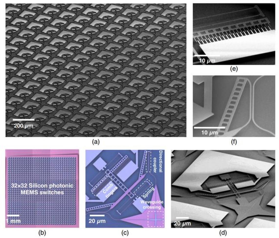
Fabricated silicon photonic MEMS switches. (a) Perspective SEM image of the fabricated silicon photonic switch array. (b) Optical microscope image of the fabricated device. (c) Optical microscope image of the switch unit cell. In each unit cell, there are 2 pairs of the directional couplers, 4 folded springs, 44 pairs of comb fingers, and 1 waveguide crossing. (d) SEM image of the switch unit cell. (e) SEM image of the comb drive and spring. (f) SEM image of the directional coupler.
Scientists in Korea, the US and Switzerland have joined forces with a metal-oxide semiconductor foundry in California to successfully mass-produce optical switches. The details were published in the Journal of Optical Microsystems and could lead to faster, more energy-efficient communication between devices in data centers.
Scientists are looking for ways to improve the speed and efficiency of communication between large numbers of high-performance computing devices inside data centers and cloud hyperscalers, especially with the escalation of artificial intelligence and machine-learning workloads.
Devices in these centers communicate with each other through a switch, which receives light-encoded messages from many devices that are then forwarded to other specific devices in the network.
Currently, this is done with electrical switches that convert the light-encoded signal back and forth between optical- and electrical-domains. In doing so, it limits bandwidth and requires additional energy.
So, scientists have been developing switches that can route light signals directly, rather than electric signals. But they have found it difficult to make optical switches large enough to handle many devices, because the larger the switch, the more light it loses.
A multinational team of scientists, including robotics engineer Sangyoon Han of Korea’s Daegu Gyeongbuk Institute of Science and Technology (DGIST), previously developed a promising optical switch. “We were certain that our switch technology could be a good alternative for electrical switches as it showed promise for mass production,” says Han.
To prove this, the researchers teamed up with the commercial metal-oxide semiconductor foundry TSI Semiconductors in California to successfully mass-produce their optical switches.
The switches were etched from silicon-on-insulator wafers. Each switch was 5.9x5.9mm in size and comprised an array of 1,024 cells with 32 input and 32 output optical waveguides. Each cell contains a double-comb-shaped actuator that moves to block or allow light through.
“This work pushes the maturity of our technology to manufacturing level,” says Han. “We are now working on packaging the chips so they can be deployable and sold on the market.”